Building a quantum simulator on solid states chip
Problem. Solid-state quantum systems try to use point defects inside a crystal as stable, addressable quantum bits. The defect has to be created, located, and measured optically — often at cryogenic temperatures — so sample preparation, microscopy, optical alignment, and cryostat infrastructure all have to work together for a single measurement.
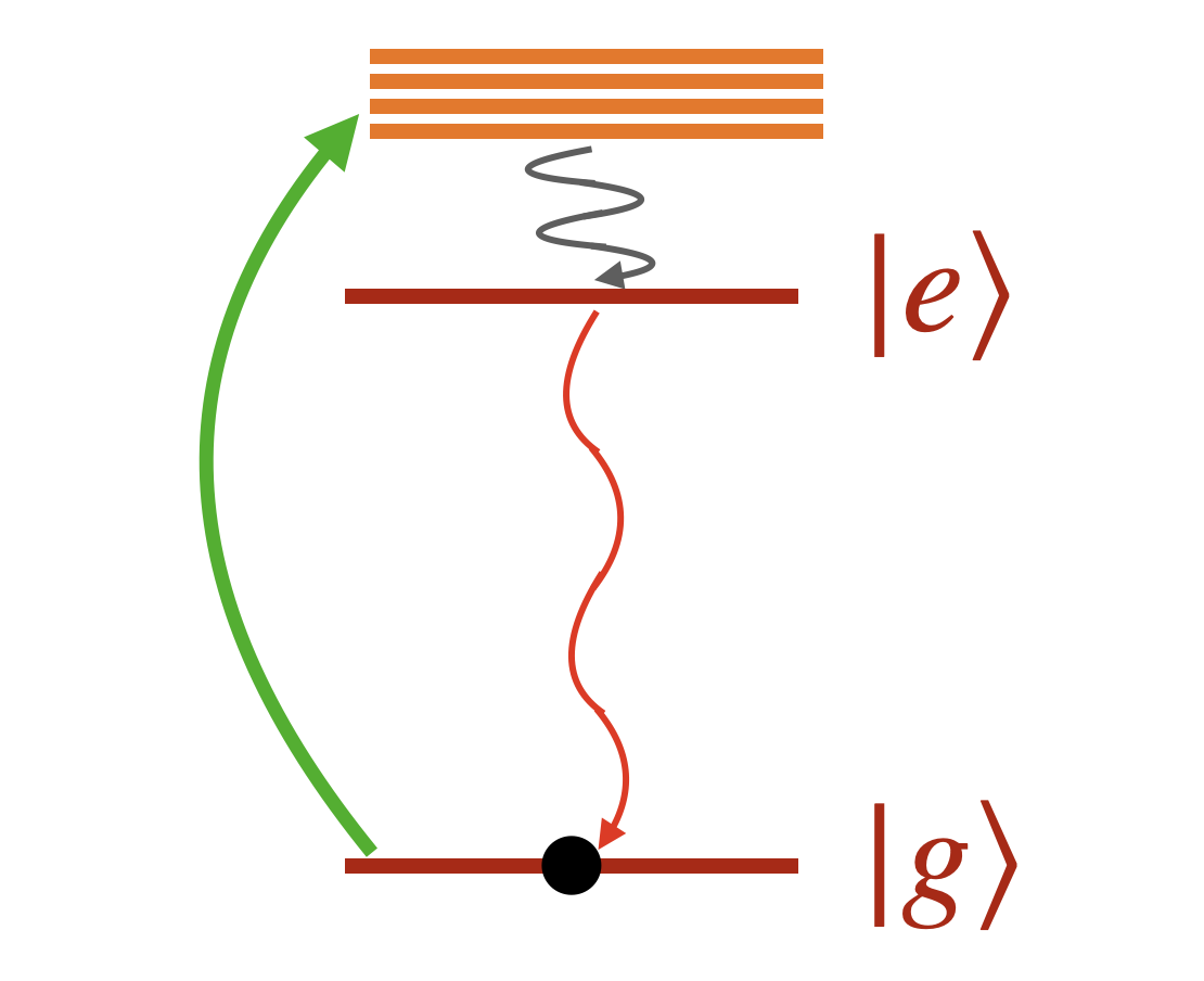
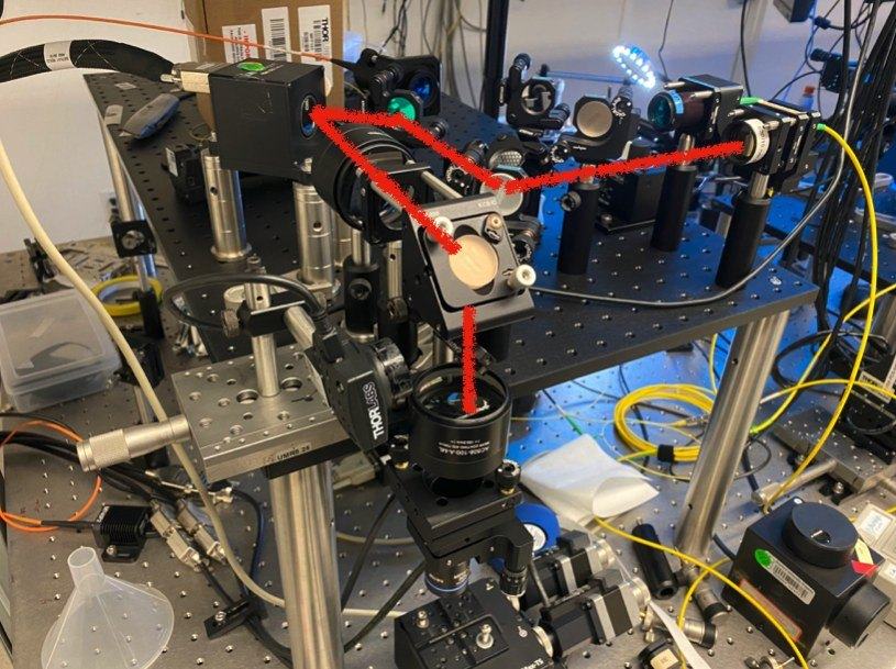
What we did. A high-energy electron beam in a TEM is used to knock out individual atoms in a silicon-carbide lattice, leaving behind vacancy defects that can act as qubits. Those defects are then addressed with a 4f confocal-microscope path that focuses excitation light onto a chosen site and collects the resulting photoluminescence; the whole measurement runs inside a cryostat so phonon decoherence is suppressed.
Result. The platform connects TEM-induced vacancy creation, confocal photoluminescence readout, and cryogenic measurement into one workflow — the standard hardware stack behind solid-state quantum experiments — with each stage chosen to keep the next stage's signal intact.
Why it matters. Silicon-carbide vacancies are one of the more practical solid-state qubit candidates: SiC is a technologically mature semiconductor, the relevant defects have long coherence times, and the optical addressing wavelengths are compatible with existing photonic infrastructure. That combination makes SiC a strong path toward scalable, fab-compatible quantum hardware.